The Optical Networking Ecosystem, Explained
A field guide for anyone trying to understand silicon photonics, the OFC conference, and why this $20 billion industry is about to get a lot more interesting.
Every March, roughly 12,000 engineers, executives, and investors descend on a convention center for OFC - the Optical Fiber Communication Conference. It's the one event where the entire optical networking supply chain collides under one roof. Laser physicists sit next to hyperscaler procurement leads. Module company CEOs share panels with Wall Street analysts. And somewhere in between, a growing wave of silicon photonics startups are trying to rewire how light moves data.
If you're new to this world, it can feel impenetrable. The acronyms alone could fill a dictionary: SiPh, CPO, DSP, PIC, QSFP-DD, OSFP, PAM4, coherent, pluggable, co-packaged. But underneath the jargon is a surprisingly clean supply chain with clear layers, clear players, and clear dynamics. This guide is an attempt to map it.
The supply chain, layer by layer
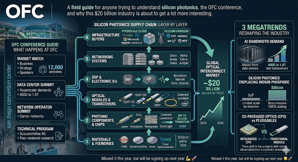
Optical networking has a vertical structure similar to semiconductors. Raw materials go in at the bottom, finished infrastructure comes out at the top. Six layers, each with its own set of companies, its own economics, and its own set of concerns.
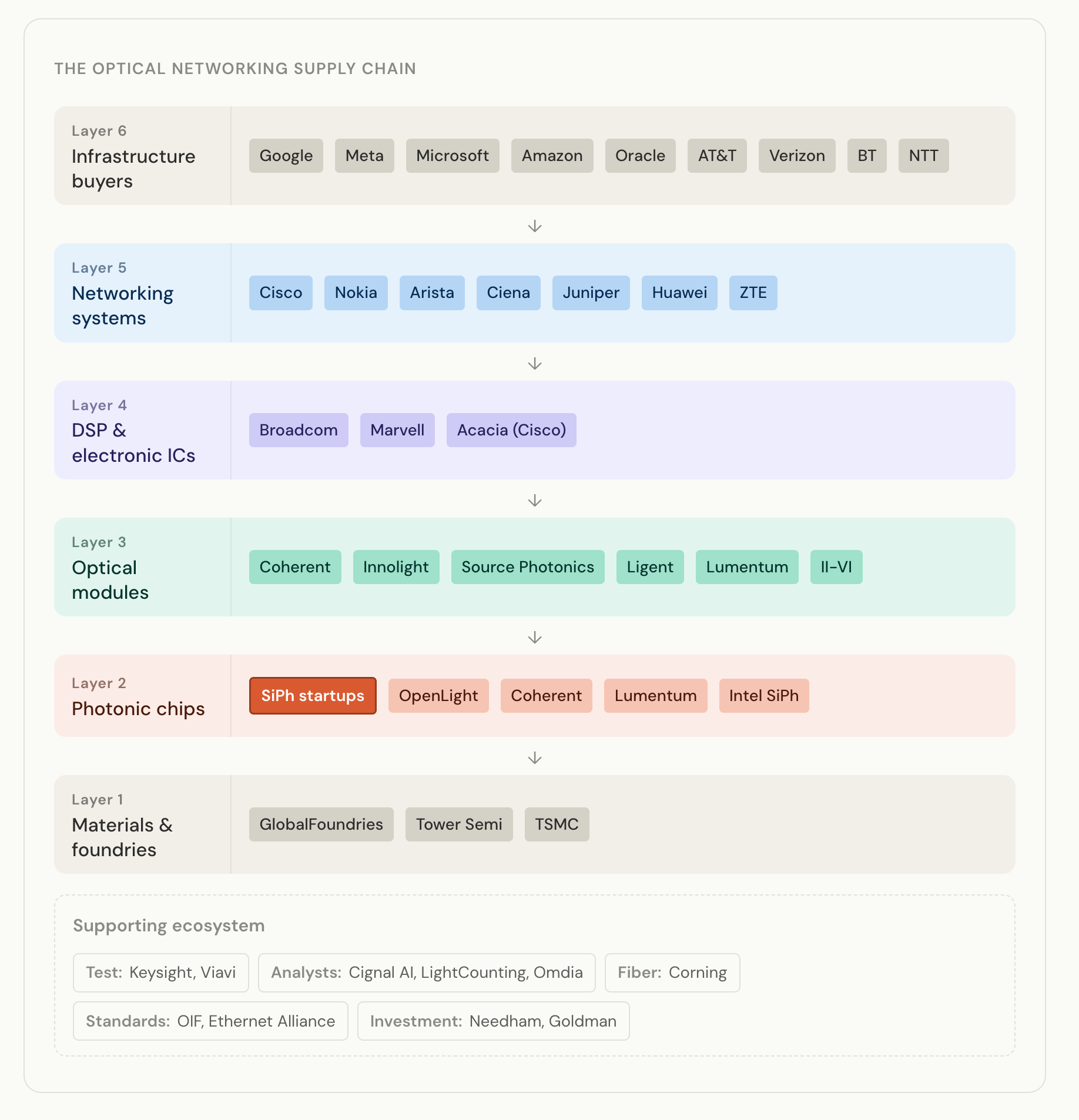
Layer 1: Materials and foundries. At the base of the stack are the fabs that manufacture the chips - both electronic and photonic. Companies like GlobalFoundries, Tower Semiconductor, and TSMC produce the silicon wafers that photonic chips are built on. This layer operates on semiconductor economics: massive capital expenditure, long lead times, and razor-thin margins that only work at enormous scale.
Layer 2: Photonic components and chips. This is where the magic happens. Companies at this layer design and build the photonic integrated circuits (PICs) that generate, modulate, and detect light. This includes lasers, modulators, photodetectors, and waveguides - the core building blocks that make optical communication possible. Historically, these components were built on exotic materials like indium phosphide (InP). Today, a growing number are being built on silicon using standard CMOS fabrication processes. That shift from InP to silicon is the heart of the silicon photonics revolution. Key players include Coherent, Lumentum, OpenLight, and Intel's silicon photonics group, alongside a new generation of startups.
Layer 3: Optical modules and transceivers. The components from Layer 2 get packaged into pluggable modules - small, hot-swappable boxes that slot into networking equipment. These transceivers convert electrical signals to light and back again. If you've ever looked at the back of a network switch and seen rows of small rectangular modules with fiber cables plugged in, those are transceivers. Companies like Coherent, Innolight, Source Photonics, Ligent, and Lumentum dominate this space. The module makers are the direct customers of Layer 2 component suppliers.
Layer 4: DSP and electronic ICs. Inside every optical module sits a digital signal processing (DSP) chip that cleans up and processes the signal. These chips are extraordinarily complex, handling modulation formats, error correction, and signal equalization at speeds that would have been unthinkable a decade ago. Broadcom, Marvell, and Cisco (through its Acacia acquisition) are the major players. The DSP companies have enormous influence over what photonic components the module makers use, because the DSP and the photonic chip have to work together as a system.
Layer 5: Networking systems. The modules plug into switches, routers, and optical line systems built by companies like Cisco, Nokia, Arista, Ciena, and Juniper. These are the boxes that actually move packets and wavelengths across data center fabrics and wide-area networks. Systems companies define the form factors, power budgets, and performance specs that ripple down through every layer below them.
Layer 6: Infrastructure buyers. At the top of the stack are the organizations that buy and deploy all of this equipment. Two distinct groups live here. Hyperscale cloud providers - Google, Meta, Microsoft, Amazon, Oracle - buy optical modules by the millions for their data centers. Telecom carriers - AT&T, Verizon, BT, NTT - buy systems for long-haul and metro networks. The hyperscalers have become the dominant force in the market, and their purchasing decisions shape the entire supply chain.
Around these six layers sits a supporting ecosystem: test and measurement companies (Keysight, Viavi), market research firms (Cignal AI, LightCounting, Omdia), fiber and connector manufacturers (Corning), standards bodies (OIF, Ethernet Alliance), and investment banks that cover the sector (Needham, Goldman Sachs).
What happens at OFC
The conference itself is structured to serve different audiences within this ecosystem. Understanding the tracks helps explain why certain people show up and what they're there to accomplish.
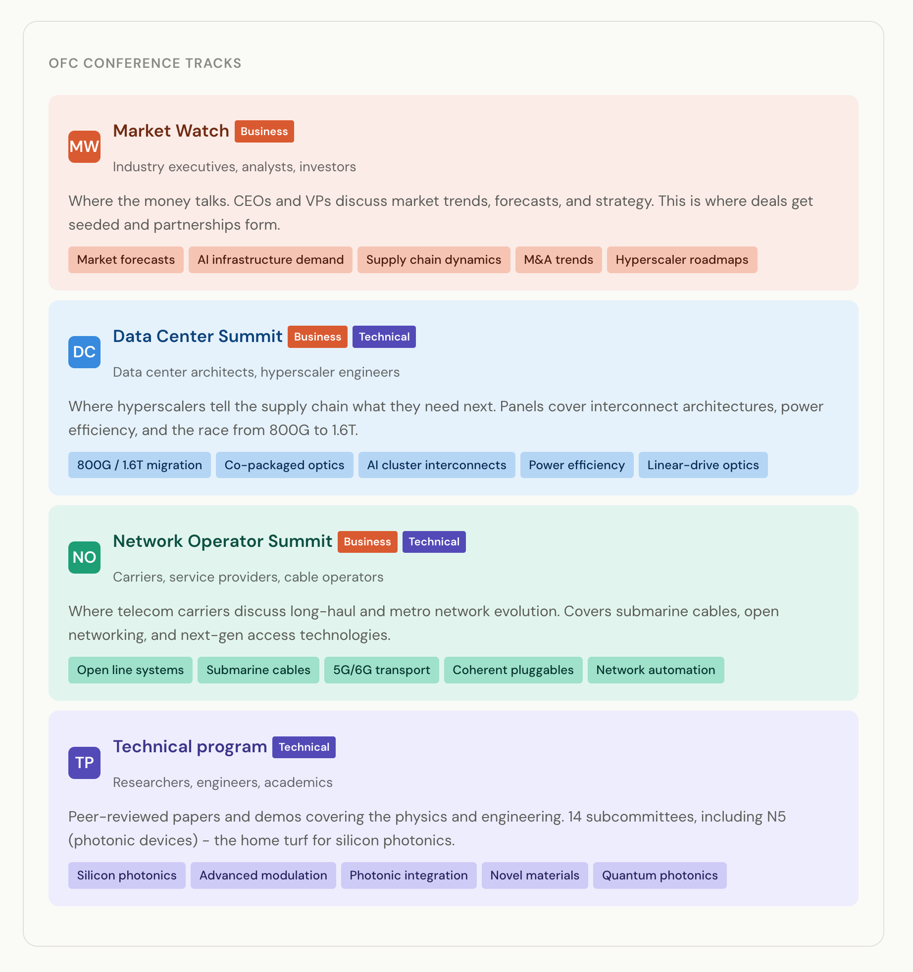
Market Watch is the business track. Industry executives, analysts, and investors gather to discuss market trends, forecasts, and strategy. This is where CEOs of module companies share revenue outlooks, where analysts from firms like Cignal AI present their market sizing data, and where deals get seeded over coffee between sessions. If you want to understand the commercial dynamics of the industry, Market Watch is where you go.
The Data Center Summit sits at the intersection of business and technology. This is where hyperscaler architects tell the supply chain what they need next. Panels cover interconnect architectures, power efficiency targets, and the migration from 800G to 1.6T data rates. For anyone building components or modules for data center applications, the DCS is essential - it's where you learn what your customers are going to demand in 18 to 24 months.
The Network Operator Summit serves a similar function for the carrier side. Telecom operators discuss long-haul network evolution, submarine cables, open networking, and next-generation access technologies. The dynamics here are different from data centers - longer product cycles, more conservative procurement, and different performance tradeoffs.
The technical program is the peer-reviewed research core of the conference. Organized into 14 subcommittees, it covers everything from novel photonic materials to advanced modulation formats. Subcommittee N5, which focuses on photonic devices and integration, is particularly relevant for silicon photonics companies. Getting a paper accepted at OFC is a significant signal in the research community.
The people who speak at the business tracks - Market Watch, DCS, and NOS - tend to be VPs, CTOs, directors, and analysts. They're the ones shaping purchasing decisions, setting product roadmaps, and brokering partnerships. The technical program draws more researchers and engineers. Both populations are valuable, but if you're trying to understand the commercial landscape, the business-track speakers are the ones to watch.
Three megatrends reshaping the industry
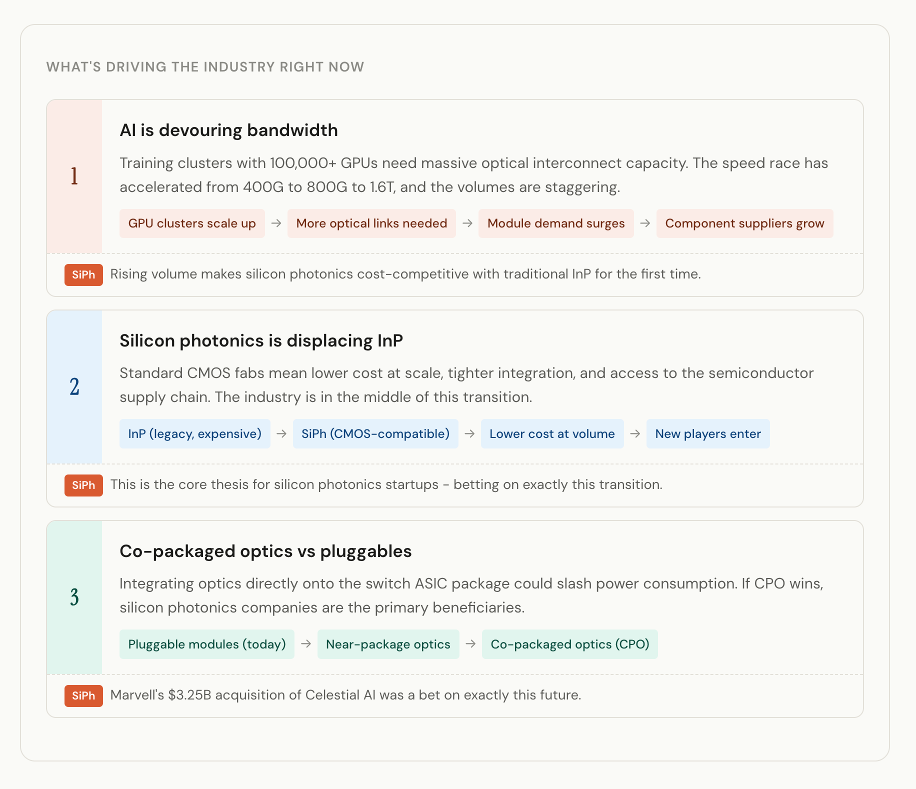
Several technology shifts are converging right now that make this an unusually dynamic moment for optical networking. Three in particular are worth understanding.
AI is devouring bandwidth
The buildout of AI training and inference infrastructure has fundamentally changed the demand picture for optical interconnects. Training clusters with 100,000+ GPUs require massive optical bandwidth between racks and between buildings. The speed race has accelerated from 400G to 800G to 1.6T transceivers in a compressed timeline, and the volumes are staggering. Hyperscalers that barely thought about optical modules five years ago are now spending billions on them annually.
The global market for optical interconnects has roughly doubled since 2020 to nearly $20 billion, and industry forecasts suggest it could double again by 2030. For photonic component suppliers, this volume surge is transformative - it means silicon photonics, which has always been positioned as a "wins at scale" technology, is finally reaching the scale where its cost advantages become decisive.
Silicon photonics is displacing indium phosphide
Traditionally, the photonic components inside optical modules were built on indium phosphide (InP) or gallium arsenide (GaAs) - exotic III-V semiconductor materials that require specialized fabs, have limited wafer sizes, and don't benefit from the decades of process optimization that silicon has undergone.
Silicon photonics takes a different approach: build the optical circuits on standard silicon wafers using CMOS-compatible fabrication processes. The advantages are significant. Silicon wafers are larger (300mm vs 100mm for InP), the fabrication tools are more mature, the supply chain is deeper, and the potential for integration with electronic circuits is much greater. The tradeoff is that silicon is an indirect bandgap material, meaning it can't efficiently generate light on its own - you still need a III-V laser source bonded or coupled to the silicon chip.
This transition is well underway. Intel pioneered commercial silicon photonics for data center applications. Cisco's acquisition of Acacia Communications for $4.5 billion in 2021 was partly a silicon photonics play. Broadcom has built significant silicon photonics capability internally. And a new generation of startups is pushing the technology further, tackling problems like integrating laser sources directly on the silicon chip and developing novel modulator architectures.
Co-packaged optics vs pluggables
Today, optical modules are pluggable - they're physically separate units that slot into the front panel of a networking switch. This architecture has been incredibly successful because it decouples optical and electrical innovation cycles and allows customers to upgrade optics without replacing switches.
But as data rates climb and power budgets tighten, the industry is debating whether optics should move closer to the switch ASIC. "Co-packaged optics" (CPO) would integrate photonic chips directly onto or adjacent to the switch package, potentially cutting power consumption by eliminating the electrical traces between the switch chip and the optical module.
CPO is contentious. The pluggable module industry has enormous momentum and a mature supply chain. Co-packaged optics would require entirely new manufacturing processes, different photonic chip architectures, and new approaches to testing and serviceability. But if CPO succeeds, silicon photonics companies are the primary beneficiaries - the tight integration required plays directly to silicon's strengths.
Marvell's acquisition of Celestial AI for $3.25 billion in early 2025 was one of the largest bets on this future. Celestial AI had developed a photonic fabric technology that uses light to move data between chips, and Marvell's interest signals that at least one major player believes co-packaged and near-packaged optics will be central to next-generation AI infrastructure.
Why this matters for silicon photonics
For companies building silicon photonic components and chips, the convergence of these three trends creates a once-in-a-generation opportunity.
The AI-driven volume surge means that silicon's manufacturing cost advantages finally kick in. When you're making millions of units, the economics of large silicon wafers and mature CMOS processes become overwhelming.
The InP-to-silicon transition means the technology is proven and the major players are investing heavily. This isn't a speculative bet on a lab curiosity - silicon photonics is shipping in volume today, and the question is how fast it takes share, not whether it will.
The CPO debate means there's a potential architectural shift that could reshuffle the competitive landscape. If optics move onto the package, the companies that can deliver tightly integrated silicon photonic chips will have a structural advantage.
For outsiders looking at this space - whether as investors, potential partners, or just curious technologists - OFC is the place where all of these threads come together. It's where the supply chain negotiates its future, where startups get noticed by potential customers, and where the industry's direction gets set for the year ahead.
Missed it this year, but will be signing up next year 💪 🚀